
Apple makes interesting chips for its mobile devices, but it doesn't talk about them much aside from extremely high-level relative performance comparisons. That means it's up to experts like the ones at Chipworks to open them up and figure it out, and they've partnered up with AnandTech to dig into the A9X in the iPad Pro.
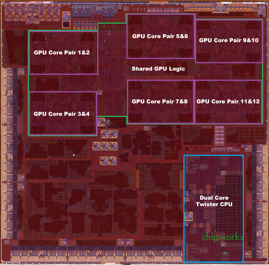
The most significant news is about the GPU, which is a 12-core Imagination Technologies PowerVR Series 7XT design. The company doesn't generally offer a 12-core design, as shown in the chart below, but the architecture is designed to be easily scalable, and it wouldn't be the first time Apple had gotten something from a supplier that other companies couldn't get. The standard A9 in the iPhone 6S and 6S Plus uses a 6-core version of the same GPU. Apple feeds that GPU with a 128-bit memory bus, something it also included in other iPads to boost memory bandwidth and GPU performance.

Imagination's chart for the Series 7XT GPU puts a hypothetical 12-core design in the same general performance neighborhood as an Nvidia GeForce GT 730M, a low-end discrete GPU that's a bit slower than the stuff Apple is shipping in its high-end MacBook Pros. Our own graphics benchmarks place it a bit higher than that, but as some of you have pointed out, iOS may have a small advantage in some of these tests because of differences between the mobile OpenGL ES API in iOS and the standard OpenGL API used in OS X.
Chipworks also notes that the A9X it looked at was manufactured on TSMC's 16nm process, and the die measures a relatively large 147mm squared (compared to roughly 128mm squared for the A8X and 104.5mm squared for the TSMC version of the A9). Apple is dual-sourcing the A9 from both Samsung and TSMC, and it could be doing the same thing for the A9X, but as AnandTech points out the A9X is going to be a much lower-volume part. In that light, there's no real need to put in the extra work required to make it on more than one process.
One final oddity of the A9X design is that it doesn't seem to include an L3 cache, the small bit of memory used in the A9 chips (as well as the A7-series, A8-series, and many CPUs from many other companies) to save the CPU and GPU some trips out to the main system memory. AnandTech speculates that a larger L2 cache, faster LPDDR4 memory, and the wider 128-bit memory bus could all have sped things up enough to reduce the need for an L3 cache.
reader comments
94