 At Hot Chips 26, AMD gave a very high level overview of the new Seattle ARM SoC. This interminable launch drip is far past annoying, a bullet point or two doesn’t justify a release to SemiAccurate anymore.
The main talk was more of a reading of bullet points, all the specs you would care about were absent. That said there are high level diagrams and charts that you might find interesting, some of which are new some previously disclosed. Lets take a look at what Seattle brings to the table, non-specifically of course.
About as much detail as AMD gave out
As you might recall when AMD first talked about Seattle over a year ago, there were no details. Then they pre-announced sampling with again no details but by then everyone knew it was an 8-core A57. By the time we got to “Core Day” last spring, 8MB cache, 28nm Globalfoundries production, and shared a package and uncore with x86 parts were out in the open. In short, Seattle was exactly what SemiAccurate told you would happen in a Jem of a story over three years ago.
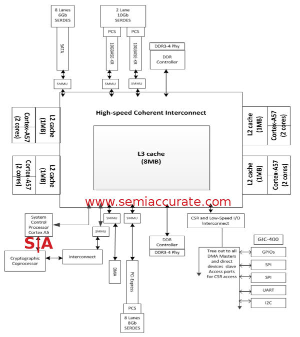
So what is the new news? Details really, but not the ones you want. Seattle will use two channels of DDR3 or DDR4, system designers choice, but it is all ECC protected. Both channels are interleaved and speeds of up to 1866MHz are supported, two DIMMs per channel, 128GB max per socket. For memory protection there is SECDED but no advanced features like chipkill or other high-end RAS, about what you would expect for a single socket SoC.
The cores themselves are pretty boring, you will have to wait for AMD’s K12 core in two years for real interesting changes. Right now there are eight A57s arranged in pairs in with a shared 1MB L2 cache and an AMBA5 CHI link to the rest of the system. All four core pairs share a single 8MB L3 for the system cache, all lines are 64B in line size. L1I is 48K 3-way associative, the 32K L1D is 2-way but ECC protected. Both the L2s and L3 are 16-way set associative and the L3 has a snoop filter built-in. In short this is pretty conventional for an ARM server, one might even say vanilla.
I/O starts off pretty vanilla too with eight SATA3/6Gb ports and the same number of PCIe3 lanes, 1×8, 2×4, or 4/2/2 are allowed. Things get interesting when you look at the Ethernet though, Seattle has a 1GB port for management and two 10GBps links for data. What is interesting is that the 10Gbps links support 10BASE-KR, the 10Gbps for 1M over copper standard. Why is this interesting?
Remember SeaMicro nee AMD Freedom Fabric? You might recall that it uses a 10Gbps Ethernet link as it’s base transport medium, Seattle has twice that per socket. That isn’t a coincidence and strongly suggests that Seattle will not have direct Ethernet out, it will be virtualized like in SeaMicro servers. Similarly the eight SATA ports are probably meant to be dedicated one to a core for local boot.
So far everything has been what you expected from an AMD uncore coupled to ARM cores, no big surprises. There are two new bits though, or at least 1.5 new bits in the CCP and SCP, the SCP being the .5. These acronyms stand for Cryptographic Co-Processor and System Control Processor, I’ll leave it up to you to figure out which is which acronym. Lets take a look at these two in detail.
The CCP is pretty simple, according to Sean White who gave the Hot Chips Seattle talk, it is a, “Lightweight DMA engine with encryption and compression” functions. It supports AES, RSA, ECC, SHA, ZLib compression/decompression, and has a hardware random number generator. This may seem superfluous because AMD used the version of the A57 with the crypto extensions but there is a point to the CCP. Dedicated hardware is usually faster and consumes less power than a generalized CPU doing the same work. It will also free up the cores for ‘real’ work, we would expect it can encrypt and/or compress data at line rates for the 2x10GbE ports but AMD wouldn’t comment on anything remotely like performance. If you are thinking encrypted backplane, so am I. They also wouldn’t comment on whose IP it is, internal or licensed.
SCP is where the real action starts, quite literally. It is an embedded A5 CPU, more of an embedded SoC in Seattle according to the presentation. It is a boot controller, a power management system, and controls system security. In fact it is almost exactly what SemiAccurate said it would be back in 2012. In many ways this tiny spec of silicon on the die is the heart of the system, but it’s existence isn’t news.
The SCP looks like a generic I/O device to the rest of the system but it is much more than that, it has its own I/O and ROMs plus a full debug system. If you care about specifics it has ARM’s CoreSight debug hooks, Embedded Trace Macrocell, and Cross-Trigger Interface built-in. The A5 in SCP also controls TrustZone for the entire SoC and has 512K of RAM to keep tabs on secure vs non-secure pages. If you don’t recall the details, TrustZone is, greatly simplified, a way to track which pages are ‘secure’ and which are more open at the memory page level via an external controller. It can also keep tabs on who owns what, plus theoretically enforce that ownership.
Remember that 1GbE link for system management? Guess where it goes? No points for that one, sorry but it is for the SCP’s RGMII. The SCP can also control the rest of the SoC’s power states, it can power things up, down, and do so on internal or external signals. See how this would be useful for something like a SeaMicro massive cluster of shared-nothing devices? Me too.
There are the usual low-speed housekeeping I/Os to make sure things work, a GPIO controller, two SPI ports, a UART, timers, I2C, and all that stuff. A little more out-of-place is a direct bridge from the SCP private address space to the SoC’s main high-speed coherent address space. Why would it need this? The boot process.
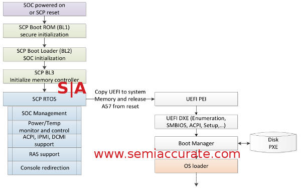
SCP secure boot process for Seattle
The system kicks off with the SCP’s A5 reading from an on-die 64KB ROM, labelled as secure and presumably actually so. That will allow the SCP to get going far enough to read an external ROM/Flash/whatever for the real boot code, UEFI 2.4 at the current time for the main SoC. Then the SCP will kick off the main memory controller allowing it to, well, use memory like it is meant to do. The SCP can then run a RTOS and do the rest of its job. For some odd reason, AMD chose a RTOS rather than Windows RT, this one seems quite puzzling. (Authors note: Yes it was a joke, it was meant to be a dig at AMD for Brazos et al choices. Everyone knows Windows RT/Win 8 is a joke, well almost everyone.)
Once all this is up and running on the SCP, it then releases the A57’s from reset and they go on their merry way. This is the normal boot process that you are probably familiar with on a normal x86 PC, and it can be an x86 PC too if AMD decides to make one. All the hooks are there and all the hooks are there, AMD just need to cut and past those cores in to the Seattle uncore. That is the point of Skybridge/Ambidextrous compute, cut and paste hopefully seamlessly.
The last question was one AMD answered quite well, essentially why would you need eight relatively weak cores on a die instead of big x86 ones? It all comes down to workloads, specifically non-cachable workloads like, oh, search and social media. If a core only needs a small code block that operates on a large data set, a low IPC core can be just as efficient as a bigger high IPC core. Why? The work is dominated by cache misses and other types of stalls, loading from main memory is key. For this a simple, cheap, and power efficient core on an SoC with lots of RAM are just the ticket. Know any potential customers with workloads like this? Me either, and yes we knew at the time, it wasn’t a guess.
In the end the new news about Seattle isn’t really news, most of it was known. Rather than give out the numbers we all wanted AMD to, they read out the feature list. Most of that was indeed new but it was fluff, the real stuff is still not public yet. While we wait for the next launch, and the one after that, and the next, we will just have to ponder why they chose this path. Especially since you can buy a dev system from their site now. SIGH.S|A
Charlie Demerjian
Latest posts by Charlie Demerjian (see all)
- Intel Announces their NXE: 5000 High NA EUV Tool - Apr 18, 2024
- AMD outs MI300 plans… sort of - Apr 11, 2024
- Qualcomm is planning a lot of Nuvia/X-Elite announcements - Mar 25, 2024
- Why is there an Altera FPGA on QTS Birch Stream boards? - Mar 12, 2024
- Doogee (Almost) makes the phone we always wanted - Mar 11, 2024