This article is more than 1 year old
IBM, Micron tag team on 3D memory breakthrough
Vertical DRAM juices bandwidth, efficiency
The Hybrid Memory Cube consortium formed by Samsung Electronics and Micron Technology this October is leveraging IBM Microelectronics' 3D wafer-baking expertise to get HMC memory to market in two years.
IBM said on Thursday that it has come up with manufacturing breakthroughs to create the conduits that link stacked blocks of DRAM, which IBM Fellow Subu Iyer will present in a paper on December 5 at the IEEE International Electron Devices Meeting in Washington, DC.
The breakthrough is significant enough for Micron to license IBM's wafer-baking techniques and to commission Big Blue to manufacture some of the necessary logic circuits in an HMC memory module.
While processors keep getting more cores and memory DIMMs keep getting fatter, keeping those cores fed with data is getting increasingly difficult because memory speeds – which are limited by the long traces between memory chips and their pins – are being held back. The answer is to stop thinking about 2D layouts for memory and to start thinking in 3D.
By stacking up memory chips, you can connect them in parallel to a logic layer and a package substrate, like the pin-out on a CPU, to build a structure that has shorter paths, can run faster, and uses less energy.
These vertical pathways are called Through Silicon Vias, or TSVs, to link DRAM chips together and to controllers that implement a crossbar interconnect that play traffic cop across the cube of memory circuits.
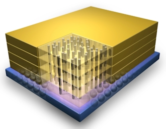
The TSVs that IBM is laying down in its manufacturing technique are copper, and integrate nicely with the high-k metal gate processes that Big Blue uses to make the embedded DRAM on its Power7 and System z10 processors. The technique can obviously be applied to standard DRAM – and in fact, Micron is using IBM's technique to make the TSV interconnects that will lash together its own DRAM chips.
The HMC logic circuits underpinning the cubes will be made using IBM's 32-nanometer high-k metal gate process from its East Fishkill, New York fab. These logic circuits will be shipped off to one of Micron's 300mm fabs in Boise, Idaho, where they will be mated with stacked memory modules and their TSV pipelines etched by Micron.
By stacking the DRAM chips in a 3D cube, the real estate in a server or PC can be significantly reduced or the memory capacity or bandwidth can be significantly increased – we all vote for the latter, of course. IBM and Micron say that HMC devices can take up about a tenth the space of traditional 2D DRAM memory sticks and require 70 per cent less energy to transfer a bit of data from the memory chip to the CPU.
The best part is that the HMC prototype modules that have been manufactured to date can deliver around 128GB/sec of bandwidth into and out of the memory block using DDR3 memory chips, compared to 12.8GB/sec for 1.33GHz DDR3 memory sticks made in a conventional 2D layout.
The HMC consortium, which includes Altera, Open Silicon, Xilinx, and now IBM, has gotten some love from Intel recently, as well, but it seems unlikely that Intel will re-enter the memory market is exited decades ago.
You could make an argument that Intel has to re-enter the memory market to justify the ever-increase costs of its fabs, El Reg supposes. It is not that much of a leap from flash to DRAM.
The consortium plans to release a spec outlining the interconnect that will enable HMC memory to be linked to GPUs, GPUs, and other components.
"This is a milestone in the industry move to 3D semiconductor manufacturing," Iyer said in a statement announcing the partnership between IBM and Micron. "The manufacturing process we are rolling out will have applications beyond memory, enabling other industry segments as well. In the next few years, 3D chip technology will make its way into consumer products, and we can expect to see drastic improvements in battery life and functionality of devices."
A spokesperson for Micron tells El Reg that prototype HMCs are already making the rounds – one was seen at Intel Developer Forum back in September – and that system makers are already indicating their interest in HMC memory. (Which kinda calls into question two-dimensional DDR4 memory, if you think about it.)
Micron expects to have HMC memory ready for sale in the second half of 2013, with server makers at the top of the list and with it eventually trickling down to PCs and other electronics. ®
