As the launch of Apple's iPhone X approaches tomorrow, eager users are set to enjoy battery life normally reserved for Apple's Plus-size form factors in a phone more closely resembling a non-Plus variant in its dimensions. The reason for this advancement is not an energy density development, but rather a smaller printed circuit board (PCB) inside the iPhone X, according to a February report from KGI Securities.
深圳的朋友拆了,還真的兩個電池 pic.twitter.com/7wzrBLVsFy — Anson Chen ☂ (@AnsonChen) November 2, 2017
This smaller PCB is thanks to a technology referred to as substrate-like PCBs, or SLP. Depictions from the report show a PCB with more layers than a traditional iPhone PCB thanks to application processor and RF signal-chain dedicated PCBs married via an interposer, creating a layer stackup nearly twice that of a conventional iPhone PCB.
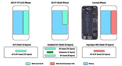
However, this doesn't come close to telling the whole story. While a new PCB stackup may offer some more flexibility in component placement, it's important to remember that the opposite side of the board from the A11 isn't empty in an iPhone 8. There are plenty of components there too — the NFC chip, display drivers, Wi-Fi combo chips, and power management ICs have all often found their homes directly opposite the workhorse application processor.
After all, 4.7-inch iPhones and their 5.5-inch "Plus" siblings have similarly sized PCBs, with battery capacity suffering as a direct result in the smaller phones. Herein lies the real problem in trying to improve battery life in these smaller form factors.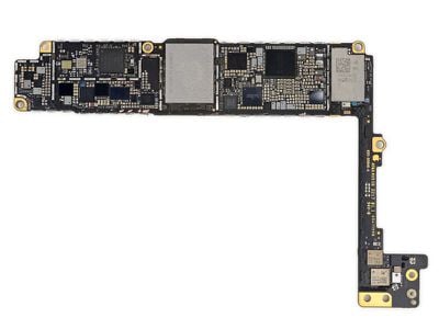
Reducing Component Footprint
To make the iPhone X PCB smaller, Apple had to devise a way to make the components on the PCBs occupy a smaller aggregate footprint. A quick glance at the above PCB shows that the board is densely populated with ICs and passive components. A natural first question is to ask if components can simply be eliminated.
A great candidate for simplification would be the RF chain. Indeed, previous iPhones have seen up to four variants for different carriers around the globe as they featured switches, filters, and amplifiers focused on the specific bands needed for these region-specific carriers. The number of variants has dwindled over the years to the current number of two and have been distilled into one model that has CDMA network capability and one that doesn't.
By supporting fewer bands per model across more models, Apple could reduce the overall size of the RF chain and save board space. A glance at the iPhone X tech spec page will show you that's not what Apple has done, as it supports the same exact bands as the iPhone 8 models across two versions.
Thus we have to look elsewhere than the RF chain for component reduction. Another way to reduce component size would be to press IC suppliers to shrink their own packages. The best example of this may be the original MacBook Air, where Intel provided a smaller package for the CPU to help Apple hit its at-the-time tiny form factor.
If a supplier were to do this, it would certainly make sense to include it in the iPhone 8 or 8 Plus as well, so there would be expected to be some sort of cost or volume pressure on the component preventing it from being more pervasive. An example might be a package that includes an interposer, which are expensive interconnect structures that allow multiple high-density pinout devices to be housed within the same package. This is the very same concept that is said to be used to mate the RF and main digital boards within the iPhone X.
The concept of moving multiple components into the same package is not new. Most of Apple's A-series chips have stacked DRAM inside of them, and Apple has made efforts to reduce package size with TSMC's InFO packaging. The Apple Watch employs an even more integrated approach with its System-in-Package (SiP) solution, including a variety of active and passive components within the same lidded enclosure. This is the direction of mobile devices in general.
Deciding whether to house components on a multi-layered PCB or push the level of integration to on-package, or even on-die, is a careful weighing of cost, space savings, and performance impacts. Moving things on-package generally improves performance as signal routes become shorter and require less power to run, but at the expense of things like more complex packaging and substrate solutions.
Putting circuits on-die provides the ultimate performance benefit, but increases die size, which can affect component yield and ultimately cost. The key with a lot of these concepts is understanding that SLP in itself doesn't really help.
Substrate-like PCBs
When component manufacturers refer to new PCB technology as substrate-like PCBs, they are referring to the interconnect density afforded by the substrates found within IC packages. Pushing feature sizes down to as little as 15 microns, these new PCB types help to get interconnect density to rival IC packages. This is really helpful for high-density routing like memory or PCI busses. Squeezing more routes in on a layer, along with smaller via features also similar to package substrates, will ultimately help to use fewer layers to route a PCB.
An iPhone X's memory is, however, already integrated into the package, and it doesn't have wide, high-speed data interfaces like you'd find in a traditional desktop platform. Thus, this is likely not the main innovation directly benefitting the iPhone X. The interposer between boards is likely helping out here.
The interposer will allow the digital and RF boards to essentially be designed separately, before being interconnected by the interposer that sits in between them. This type of multiple step approach is common in PCBs, as they often start with non-conductive cores which are then built up with successive metal and dielectric layers, letting the fabrication house add small vias layer by layer for a complex PCB. The interposer extends this concept by integrating an ever tighter interconnect pitch, normally reserved for device packages, and greatly inflating cost.
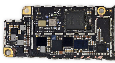
This separate PCB approach will help Apple achieve better isolation between its digital and RF circuit sections. Indeed, close inspection of an iPhone PCB will show dashed-looking lines separating circuit types from each other. The above image shows the audio and RF sections separated on an iPhone 8 Plus PCB.
Separating these components is important, as interference from neighboring components can cause things like decreased dynamic range in analog and RF circuits, or compromised signal integrity in digital circuits. As a consumer device, radiated signals are also a concern. Apple made efforts to increase self-compatibility and standards compliance when it patented and subsequently introduced and improved sputtered coatings for chips found in its mobile devices.
All of these steps help Apple to place components closer together, and it offers more freedom in where to place them in proximity to each other. However, the board space is still largely consumed. Aggressive efforts may claim perhaps up to 10 percent of the board space back, but more is needed to significantly cut down PCB size. Apple's engineers need to exploit more than just the X and Y dimensions.
3D Techniques
To truly make advances in the space needed to house all the components in the iPhone, the height of the PCBs must be leveraged as well. 3D and 2.5D IC techniques such as chip stacking, through-silicon vias, interposers and other techniques have gotten a lot of exposure in recent years for device packaging, but they can also apply to PCBs to some extent. PCB vendors have been embedding simple passive components such as resistors, capacitors, and inductors in PCBs for years.
These features were first intrinsic to the process, whether through resistor films, printed winding traces, or using the PCB dielectric as the foundation for a capacitor formed across layers. Embedded physical components are now rising in prominence, with vendors even planning for embedded active components in the not too distant future.
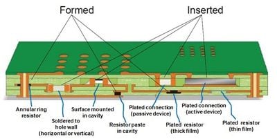
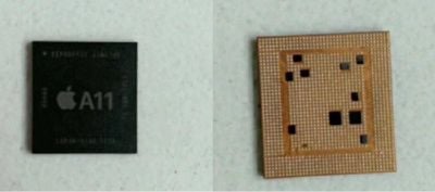
Though it has gone somewhat unnoticed, Apple has already been employing this technique with its A-series application processors. Several years ago, leaked packaged parts began to show curious voids on the underside where the normal interconnect array would be expected. These voids are likely spaces for passive filtering components to nestle inside the package.
This achieves two things. First, it decreases the amount of board space needed to seat all components. Second, it often carries a performance advantage because proximity to the metal inside the device is one of the key performance drivers of active devices such as this.
The capacitors and inductors used to filter and bypass the power on the application processor serve to prevent voltage droop in changing current demand scenarios, as well as provide a bypass route to ground for high frequency noise. Placing it as close to the device as possible cuts down on unwanted parasitics which reduce these components' effectiveness.
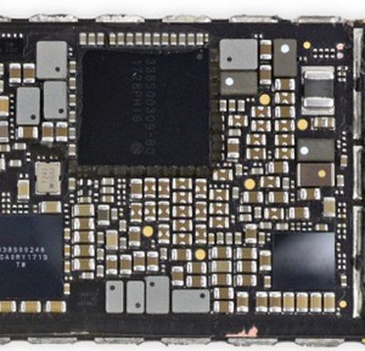
By extending this concept to PCBs, Apple can utilize any extra space within the PCB to house these components. Examination of the rear of an iPhone 8 Plus PCB shows there are numerous passive components sitting on the rear of the PCB behind the A11.
The more of these components that can be embedded within the board stackup, the more space efficiency the design can have. At an extreme, the PCB would have these components untouched, with an interposer (or perhaps multiple, interspersed with bonding material to match the boards) having a cutout in this area so that the digital and RF boards could be laminated together. This concept in itself presents technical challenges, and a gradual adoption rather than a momentous shift should be expected for embedded components.
What should be clear moving forward is that the internals of PCB stackups could prove to be just as interesting as their surfaces and the x-ray shots of component dies that we have come to expect. Perhaps we'll get a glimpse at some of these concepts once the teardowns start rolling in.


Top Rated Comments
I dunno why
Silly, I know